Features

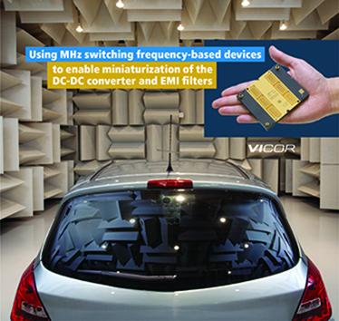
MHz switching frequency-based devices enable miniaturization of the DC-DC converter and EMI filters
Achieving EMI conducted emission compliance for automobiles with a single stage filter. By Nicola Rosano, Sr. Strategic FA/System Engineer at Vicor
More details...
AC/DC power factor correction module offers up to 1,512W
A full brick package developed by TDK-Lambda, the PF1500B-360, is for high voltage distributed power architectures
More details...
A full brick package developed by TDK-Lambda, the PF1500B-360, is for high voltage distributed power architectures
More details...
Power Electronics Europe News
Embedded GaN Power Converter
Embedded GaN Power Converter
Fraunhofer IAF has developed a fully integrated monolithic multilevel converter in high-voltage AlGaN/GaN-on-Si technology. The integrated inverter circuit on an area of just 2 mm × 3 mm is designed for maximum voltage of /- 400 V and current of 5 A, it comprises four transistors and six diodes. The circuit exhibits minimal dynamic losses at very high frequencies. The excellent switching performance was demonstrated with a test setup on the basis of the ECP® technology from AT&S.
A corresponding test setup is necessary in order to evaluate the chip. The packaging of the dies constitutes a key factor in this regard. If lateral components are employed, the source, drain and gate pads are on one side and the back of the die is used for heat dissipation. Since the conventional approach with wirebonds imposed restrictions, with the ECP® the power components are embedded into the PCB material and can be connected from both sides. The chips are connected directly via copper-plated microvias.
This permits low impedance connections and significantly lower inductances compared with wirebond technology. The rear of the die is also connected by means of copper-plated microvias. This ensures excellent heat dissipation. “We are highly impressed with the technology from AT&S and see this mounting technology as opening up entirely new possibilities – particularly also for more complex monolithic integrated GaN power circuits, as used on our multilevel converter chip. With a conventional design, we were hardly able to use and/or evaluate the powerful chip," Richard Reiner, scientist at Fraunhofer IAF, stated. “Power electronics constitutes a major field of application and focus for our embedding technology. Particularly for the use of 'wide bandgap semiconductor' materials, such as GaN, the embedding technology makes innovative miniaturized power packages possible for higher efficiencies, enhanced thermal performance and higher power densities. In collaboration with partners, AT&S has for example already implemented various GaN power circuits, which are characterised by excellent switching performance and high efficiency”, emphazised Dietmar Drofenik, CEO of the Business Unit Advanced Packaging at AT&S.
AT&S (Hall 6, Stand 323) and Fraunhofer IAF (Hall 7, Stand 237) at PCIM
www.ats.net
| Home / News / Features / Events / Media Data / Issue Archive / Magazine Subscription / Contact Us
| Privacy Policy | Site Map | © Copyright DFA Media
| Web design by Immersive Media
| Privacy Policy | Site Map | © Copyright DFA Media
| Web design by Immersive Media


