


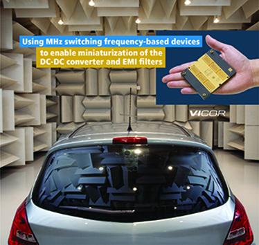
MHz switching frequency-based devices enable miniaturization of the DC-DC converter and EMI filters
Achieving EMI conducted emission compliance for automobiles with a single stage filter. By Nicola Rosano, Sr. Strategic FA/System Engineer at Vicor
More details...
A full brick package developed by TDK-Lambda, the PF1500B-360, is for high voltage distributed power architectures
More details...
 Topside cooling enables engineers to use conventional PCB cooling techniques when incorporating the semiconductors into designs for products such as inverters, UPS, hybrid electric vehicles/electric vehicles, high voltage DC/DC conversion and consumer products.
The GaN transistors are based on the company’s proprietary Island Technology. The die consist of islands rather than traditional fingers, which brings advantages in terms of current handling, lower inductance, scaling, isolation and thermal management. It also enables smaller die and lower cost, says the company. The enhancement-mode devices with current ratings ranging from 8.0 to 250A are delivered in a proprietary GaNPX packaging, where the die is embedded within a laminate construction. A series of galvanic processes replace conventional techniques such as clips, wire bonds and moulding compounds. The near-chipscale high power switching transistors can be cooled via the topside of the chip using a heat sink or fan. The transistors can also be cooled from the bottom surface of the die through conduction to the PCB.
View PDF
| Privacy Policy | Site Map | © Copyright DFA Media
| Web design by Immersive Media