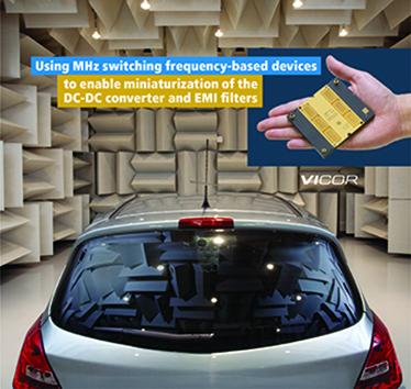
MHz switching frequency-based devices enable miniaturization of the DC-DC converter and EMI filters
Achieving EMI conducted emission compliance for automobiles with a single stage filter. By Nicola Rosano, Sr. Strategic FA/System Engineer at Vicor
More details...
A full brick package developed by TDK-Lambda, the PF1500B-360, is for high voltage distributed power architectures
More details...
 The CV,CC and CP flyback switcher ICs also eliminate DC/DC post-regulators, adds the company.
The ICs deliver up to 65W and achieve up to 94% efficiency across line and load conditions. Dynamically adjustable control of voltage (in 10mV steps) and current (in 50mA steps) is via a simple two-wire I2C interface. Devices may be paired with a microcontroller or take inputs from the system CPU to control and monitor the off-line power supply.
Applications include virtually any rapid-charging protocol, including USB Power Delivery (PD) 3.0 PPS, Quick Charge 4/4 , AFC, VOOC, SCP, FCP and other industrial and consumer battery chargers, dimmable LED ballast drivers and field-configurable industrial power supplies.
The power-conversion ICs have a microprocessor VCC supply, which eliminates the need for an external LDO to power the microcontroller. There is also an n-channel FET driver which may be used to enable or disable the main power output. Protection features include integrated bus voltage, current and fault-reporting telemetry and dynamically configurable protection such as one time programmability (OTP), line over voltage/ under voltage (OV/UV), output OV/UV, and short-circuit. These features can reduce the bill of materials and design complexity for a sophisticated offline power supply, says the company.
The IC is being introduced in response to the rapid transition in the AC/DC power conversion market, as system designers need a programmable solution that can adapt to a selection of fast-charging protocols including the recent USB PD 3.0 PPS specification. Controlling the output voltage and current of a power supply over a wide range is useful in the design of specialised applications with smaller production runs, as they can easily configure a single board design for multiple products, using software either at manufacture or during installation, points out the company. Target end applications are smartphones, notebooks, tablets, smart speakers and non-charging applications that require either a load-controlled or configurable output.
The ICs employ proprietary FluxLink, plus synchronous rectification, quasi-resonant switching and a precise secondary-side feedback sensing and feedback control circuit.
Devices are CQC certified, UL recognised and TUV (EN60950) approved to bridge the isolation barrier. The InSOP-24D package also provides a low-profile, thermally efficient solution with extended creepage (11.5mm and above) and clearance between primary and secondary sides for high reliability, surge protection and ESD robustness.
Samples are available now.
View PDF
| Privacy Policy | Site Map | © Copyright DFA Media
| Web design by Immersive Media


